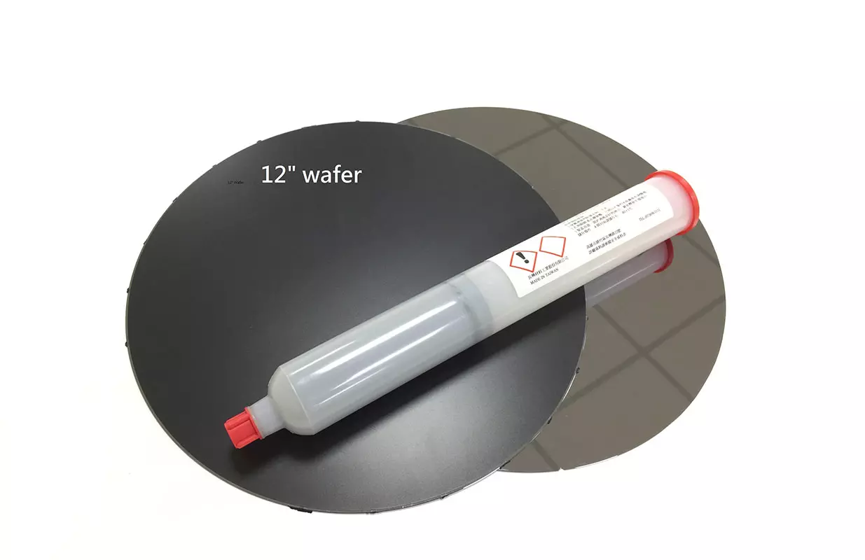
3D IC combines with different function chips into a wafer-level or panel-level package, which not only significantly reduces the product thickness, but also achieves the low power consumption requirement. It will be the mainstream of high-end packaging in the future. Wafer-level package, depending on the fab or assembling house manufacture process, can be divided into fan-in, fan-out (InFO), and Mold Under Fill(MUF) which combines capillary under fill and structure molding two process into one step.
Application products are used in big data transmission, Internet of Things (IoT), automotive electronics, and artificial intelligence (AI).